The previous computer had two 32KB RAM chips to provide a total of 64KB RAM. To run a user program you need to get it into RAM somehow, so I also included a 128KB ROM chip which occupied the lower 16KB of the Z80's address space to provide the fixed operating system that could be used to load programs. By adding memory banking hardware I could select one of eight 16KB pages of ROM. The next 16KB was one of two banks of RAM from one RAM chip, and the final 32KB was mapped directly to the other RAM chip.
This is all fairly complicated, and not very flexible. Programs written for CP/M tend to be loaded into memory starting at address $0100, which is impossible with my old design as that section of memory is taken up by ROM.
Giving another device access to the buses
The Z80 accesses memory and other hardware devices using three buses; an eight-bit data bus which shuttles bytes of data between the various chips, a sixteen-bit address bus which addresses a location in memory or a particular I/O device, and a control bus which contains numerous lines that specify the type of operation (for example, if /MREQ and /WR go low together it indicates that a byte is being written to memory, or if /IORQ and /RD go low together it indicates that a byte is being read from an I/O device).
There is also a pin named /BUSREQ that can be used to request access to these buses. The Z80 will periodically check this pin and if it is held low it will put the data, address and control buses into a high-impedance state and drive /BUSACK low to acknowledge this. This effectively removes the Z80 from the circuit, and another device can now drive the buses.
Click to toggle labels
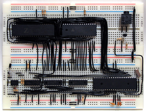
This is the feature which I have based the new design around -- the current prototype is pictured above. It features a Z80 and 128KB of SRAM (only 64KB is currently addressable) on the upper board. On the lower board is an ATmega644P microcontroller, which is used to start the computer.
When the circuit is reset, the ATmega644P requests access to the buses from the Z80. When access has been granted, it proceeds to copy the CP/M BIOS from the 512KB flash memory IC to a specific location in RAM (currently $F200). It then writes the Z80 jump instruction jp $F200 to the start of memory, returns control of the buses to the Z80 and pulses its /RESET pin. The CP/M BIOS then runs directly on the Z80.
As the ATmega644P doesn't have enough pins to drive all of the buses directly, I've added sixteen GPIO pins by using two MCP23S08 8-bit I/O expander chips. These are used to drive or sample the Z80 address bus; the data and control buses are driven or sampled directly by the GPIO ports on the ATmega644P.
Using a slow to respond microcontroller for I/O
The Z80 is most useful if it can talk to the outside world somehow, which is usually achieved by reading from or writing to I/O devices. In my previous design I built these out of latches and lots of glue logic. As I've added a powerful microcontroller to the computer which features a number of useful on-board peripherals, it would seem sensible to use that instead.
One problem with this idea is that the Z80 expects to read or write to an I/O device in a mere four clock cycles. The AVR has a delay between an interrupt occurring (such as a pin state changing) and executing interrupt service routine of at least five clock cycles. Even though the AVR is running at twice the clock speed of the Z80 this still doesn't provide much time to sample the address bus and perform some useful action before returning a value to the Z80. Fortunately, the Z80 has another useful pin, /WAIT, specifically to address this concern. By pulling this pin low the Z80 can be stalled, allowing the I/O device plenty of time to respond. I have included a 7474 D-type flip-flop as an SR latch to control the /WAIT pin. When the Z80's /IORQ pin goes low the flip-flop is reset, which pulls the /WAIT pin low. When the AVR notices that the /IORQ line has gone low it samples the address bus, performs the requisite task then sets the flip-flop, which drives the /WAIT pin high again and the Z80 continues executing the program.
The 7474 is a dual D-type flip-flop, so I have used the second flip-flop to halve the AVR's 20MHz clock signal to provide the 10MHz clock for the Z80.
CP/M interacts with the host computer by calling numbered BIOS functions. I have implemented a number of these BIOS functions by outputting a value to a port number that matches the BIOS function number. For example, CONOUT is function number four and is used to send the character in register C to the console.
CONOUT: ld a,c out (4),a retThe AVR detects a write to port 4 and sends the incoming byte to one of its UARTs. I have connected this UART to a simple transistor inverter (pictured in the top right of the above photograph) and plugged the output from that into one of my PC's serial ports, so by running a terminal emulator I can see the output of CP/M on the screen. I have implemented only a handful of other functions (WBOOT outputs a value to port 1 to indicate that I should load the BDOS and CCP into RAM from the flash memory and READ can be used to copy 128 byte floppy disk sectors from flash memory to Z80 RAM) so the results are not exactly impressive:
Quote:Loading BIOS...OKLoading BDOS...OKLoading CCP...OKA>
As I haven't implemented console input yet there's no way to type at the prompt, but that it gets that far is encouraging.
I haven't implemented writing to the flash memory due to a mistake I made when reading its datasheet. When writing to flash memory the value you write is ANDed with the data that's already there (you can only set a 1 bit to a 0 bit, but not vice-versa) - this is referred to as programming. If you want to write a 1 bit you have to erase the memory before writing to it (this is unsurprisingly referred to as erasing). Flash memory can be split into pages (small regions, in this case 256 bytes) and sectors (large regions, in this case 64KB). You can often program any number of bytes (up to a page at a time, aligned to page boundaries) but can only erase in larger blocks -- pages, sectors, or the entire memory (bulk erase). I thought that the flash memory ICs I bought supported page erasing, but they only support sector erasing. CP/M transfers data between floppy disks and RAM in 128 byte floppy disk sectors, so to write an updated sector I would need to read 64KB from the flash memory, update a 128 byte region within it, erase an entire flash sector, then program the 64KB back to it. This would be very slow and quickly wear out the flash memory, so I am looking for some replacement flash memory ICs which do support page erase.
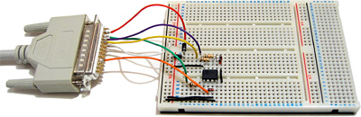
To copy the system files and a sample disk image to the flash memory I cobbled together the above parallel port programmer which is driven by an application cobbled together in C#. It's rather slow but gets the job done -- unlike my AVR programmer. After finally managing to get CP/M to boot in a satisfactory manner I made a few tweaks to the AVR program and hit the "Build and Program" button in the editor. The code built, but rather than program the AVR my computer switched off. No error message, not even a blue screen, just a sudden and surprising power down. Since then I've only managed to talk to the AVR once; every other time has resulted in either a power down or blue screen. I had hoped to add some keyboard handling routines to the project to at least be able to interact with CP/M, but after fiddling around for an hour and a half without managing to get anything working again I gave up. I wish I knew why it suddenly stopped working, after hours of reliable service -- maybe it's a hint that it's time to buy a proper USB debugger rather than the cheap and cheerful home-made serial port programmer I've been using!
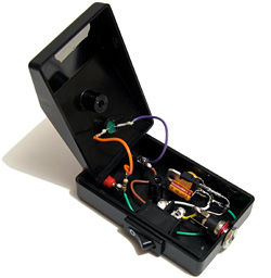
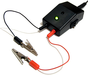
One equally cheap but useful addition to my tools is the above 5V power supply (yes, it's just a 7805 regulator in a box). Every project I have built needs a 5V supply from somewhere, which usually comes from a 7.5V wall wart power supply unit regulated to 5V with a 7805. This takes up valuable breadboard space and the weight of the cable from the power supply tends to drag the breadboard around the smooth surface of my desk, so having a dedicated box with an on-off switch, indicator LED, reverse voltage protection and an easy way to connect to the circuit via 2mm sockets is very handy indeed.
I now need to find a way to program AVRs without my PC switching itself off before I can make any more progress on the project...