Data is stored in RAM in an array of bits called a "bank".

A horizontal line of bits make up a "word line" and a vertical line of bits make up a "bit line".
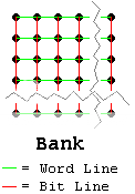
The array is split up into rows and columns. A row is equivalent to a word line, so that's easy enough. A column is made up of multiple contiguous bit lines, either 4, 8, or 16 depending on the architecture of the chip. The number of bit lines which make up a column is the word width of the chip, or just simply the "width". This is usually written with an "x" followed by the width: x4, x8, and x16.

The number of rows depends on the generation of DDR and the "density" of the chip. The density is the number of bits the chip has total across all banks. The number of columns depends on the density and width of the chip. The exact row and column counts for the possible densities and widths are specified by the DDR standard for the generation in question, although my experience is that you have to perform some calculations to find them. Here is a table I put together of the row and column counts for the first generation of DDR:

Reposted from http://invisiblegdev.blogspot.com/