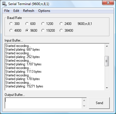
Yes, it says plating.
A single RAM chip offers 32K with an eight-bit word size. This requires fifteen lines to address it, A0..A14. The PICAXE-28X1 that is to control the circuit does not have enough output pins to be able drive this address bus and a data bus (to transfer values to and from RAM) and a still have enough pins left over to control the various components. To get around this, two octal (eight-bit) latches are used to drive the address lines, A0..A7 from one chip and A8..A14 from another. The inputs to these latches are connected to the data bus (PortC on the PICAXE), and two pins on the PICAXE are set aside to trigger the latch enable pins on either latch.
What this means in practice is that if you wished to change the current address to $1234 you would put $34 on the data bus and trigger the latch that corresponds to the least significant byte of the address, then put $12 on the data bus and trigger the latch that corresponds to the most significant byte of the address.
Any hobbyist can have wire insulation in any color that he wants so long as it is black.
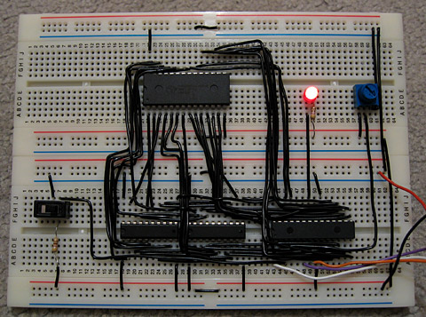
A 10K potentiometer provides the required analogue input and an LED provides the output. The switch on the left is used to change between recording and playback modes. The large chip at the top is the RAM, the two small ones in the middle are the octal latches and the medium one on the right is the PICAXE-28X1.
As only 15 lines are needed to address 32KB, the most significant bit of the address bus is wired to the /WE pin of the RAM chip. This pin determines whether we're writing to (low) or reading from (high) the chip. This effectively means that addresses $0000..$7FFF are used when writing and addresses $8000..$FFFF are used when reading.
The only remaining connections to the RAM chip required are chip enable (/CE) and output enable (/OE). When chip enable is low, the RAM chip can be accessed; when high, it ignores all input. When not in use we therefore make sure that chip enable is high. When output enable is low, the RAM chip puts the value at the current address onto the data bus, so we need to pull this low when reading but make sure it's left high most of the time so that the RAM chip doesn't interfere with other devices trying to put a value on the data bus.
The code for the test program is as follows:
; Pins:Symbol RamChipDisable = 4Symbol RamOutputDisable = 5Symbol AddressLatch0 = 6Symbol AddressLatch1 = 7; Registers:Symbol RamValue = B0Symbol RamAddress = W1 ; B3:B2Symbol RamAddressLow = B2Symbol RamAddressHigh = B3Symbol RamPointer = W2 ; B5:B4Symbol RecordingLength = W3 ; B7:B6Boot: Let DirsC = $00 High RamChipDisable High RamOutputDisable Low AddressLatch0 Low AddressLatch1 Let RamPointer = 0 SetFreq M8 Main:StartPlaying: SerTxd ("Started playing: ", #RecordingLength, " bytes", CR, LF) Let RamPointer = 0 Pause 100PlayingLoop: If PortA Pin1 = 1 Then StartRecording ; Read stored value from RAM. Let RamAddress = RamPointer GoSub ReadRam ; Set LED brightness to stored value. Let W4 = RamValue * 4 HPwm PwmSingle, PwmHHHH, %0100, 255, W4 ; Increment playback pointer and loop if hit end. Let RamPointer = RamPointer + 1 If RamPointer = RecordingLength Then RamPointer = 0 EndIf ; Loop back. GoTo PlayingLoopStartRecording: SerTxd ("Started recording...", CR, LF) Let RecordingLength = 0 Pause 100RecordingLoop: If PortA Pin1 = 0 Then StartPlaying ; Read value from ADC. ReadAdc 0, RamValue ; Set LED brightness to read value. Let W4 = RamValue * 4 HPwm PwmSingle, PwmHHHH, %0100, 255, W4 ; Store value read from ADC into RAM. Let RamAddress = RecordingLength GoSub WriteRam ; Increment record pointer. Let RecordingLength = RecordingLength + 1 GoTo RecordingLoopWriteRam: ; Set up address bus: Let DirsC = $FF Let RamAddressHigh = RamAddressHigh & %01111111 Let PinsC = RamAddressHigh High AddressLatch1 : Low AddressLatch1 Let PinsC = RamAddressLow High AddressLatch0 : Low AddressLatch0 ; Set up data bus and write: Let PinsC = RamValue Low RamChipDisable High RamChipDisable Let DirsC = $00 ReturnReadRam: ; Set up address bus: Let DirsC = $FF Let RamAddressHigh = RamAddressHigh | %10000000 Let PinsC = RamAddressHigh High AddressLatch1 : Low AddressLatch1 Let PinsC = RamAddressLow High AddressLatch0 : Low AddressLatch0 ; Set up data bus and read: Let DirsC = $00 Low RamOutputDisable Low RamChipDisable Let RamValue = Pins High RamChipDisable High RamOutputDisable ReturnAs before, there's a simple video of the circuit in action.
798KB WMV